Config Editor
This guide explains how to use a config view to control netlisting in Revolution EDA. A
config view lets you decide which cellview the netlister should use at each point in a
hierarchy, for example schematic, symbol, spice, or veriloga.
Quick Orientation
- A config view is created as a normal cellview, but its purpose is netlisting control.
- A config view is always tied to a top-level schematic view.
- The editor shows the netlister’s current view choice in View Found.
- You can override that choice per cell through the View To selection column.
File -> Updaterebuilds the configuration table from the referenced schematic hierarchy.File -> Savewrites the config view to disk.
What a Config View Does
Without a config view, the netlister follows the application’s switch/stop view rules. With a config view, you can override those defaults for specific cells in a design hierarchy.
Typical uses include:
- choosing a
symbolorspiceview instead of aschematic - stopping hierarchy traversal at a selected block
- mixing behavioural and transistor-level views in the same netlist
Typical Config Flow
- Create a new cellview whose type and name include
config.
- Choose the source schematic view that the config will control.
- Review the default switch/stop view lists. Click
OKbutton. - Open the config editor window.
- Use
File -> Updateto populate the hierarchy table. - Change View To combobox for any cells you want to override.
- Save the config view.
- When creating a netlist from the schematic side, choose the config view instead of the plain schematic view.
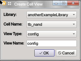
Creating a Config View
Create a config view the same way you create other cellviews in the Library Browser.
- Open the Create New CellView dialog.
- Select
configas the view type. - Enter a view name that includes
config.
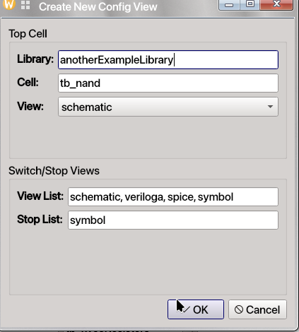
After that, Revolution EDA opens a config-specific setup dialog where you choose:
- the top-level schematic view the config is based on
- the default View List used for switch-view traversal
- the default Stop List
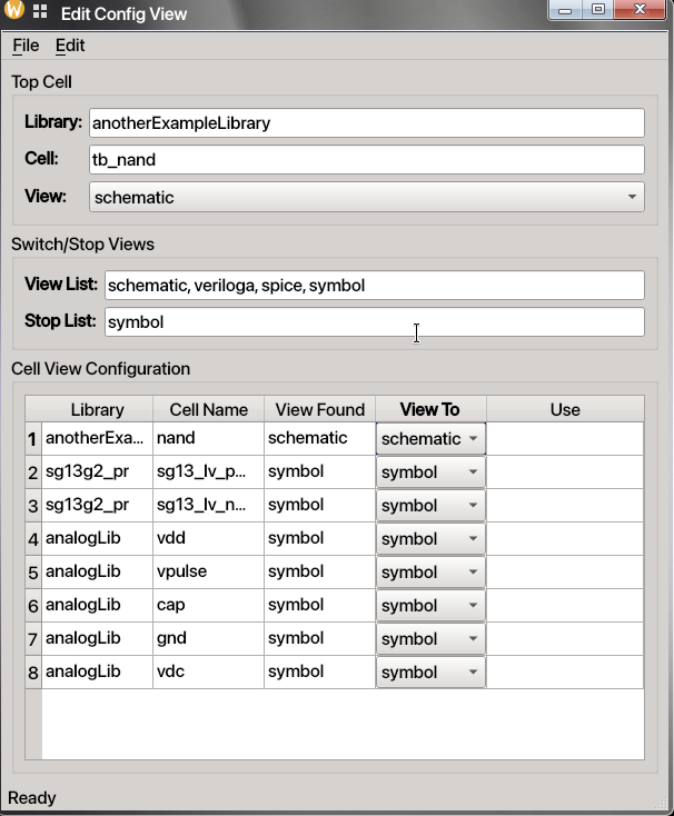
Config Editor Window
The config editor is simpler than the schematic, symbol, and layout editors. It is centered around three areas:
- Top Cell
- Library
- Cell
- Schematic view selection
- Switch/Stop Views
- View List
- Stop List
- Cell View Configuration
- one row per discovered cell in the hierarchy
- current resolved view in View Found
- chosen override in View To
The View To field is presented as a combo box for each row, so you can choose from the
allowed views already known for that cell.
Menu Actions You Will Use Most
File Menu
The config editor uses a very small File menu with only the actions required for config editing.
File -> Update: rebuilds the configuration table from the referenced schematic hierarchy.File -> Save: saves the config view JSON to disk.
File menu actions:
| Action | Shortcut | Notes |
|---|---|---|
File -> Update | None | Re-evaluates the hierarchy using the current source schematic and view lists. |
File -> Save | None | Saves the config view to disk. |
Edit Menu
The config editor currently shows an Edit menu in the menu bar, but the main user-facing
workflow is driven by the File menu and the configuration table itself.
How to Change Netlisting Behavior
There are two main ways to change what the netlister will use.
1. Change the View List / Stop List
You can edit the comma-separated values in:
- View List
- Stop List
Then use File -> Update to rebuild the configuration table. The View Found column will
change to reflect the new traversal preferences.
2. Override a Specific Cell in the Table
For each discovered cell, use the View To combo box to override which view should be used during netlisting.
This is especially useful when you want one block to netlist from:
- a symbol view
- a Verilog-A view
- a SPICE subcircuit view
- a schematic view
If you override a cell that has deeper hierarchy under it, then using Update may change the
set of rows shown in the editor because the traversal path has changed.
Netlisting with a Config View
At present, netlisting is still started from the schematic side rather than directly from the config editor window.
Typical workflow:
- Save the config view.
- Open the relevant schematic or return to it.
- Start netlist creation from the schematic editor.
- In the netlist/export dialog, select the config view instead of the default schematic-only traversal.
- Generate the netlist.
The resulting netlist follows the hierarchy choices defined by your config view.
Practical Example
Imagine a top-level schematic containing a child cell named example1.
- If
example1is mapped tosymbol, the netlister will stop descending into that block and use the symbol-level netlisting path. - If
example1is mapped toschematic, the netlister can traverse into that hierarchy and continue according to the selected views below it.
This lets you compare behavioural and transistor-level netlisting strategies without editing the original schematic hierarchy.
Compare these two actual netlists when schematic cellview or spice cellview is used for
netlisting.
**********************************************************************************
** Revolution EDA CDL Netlist
** Library: anotherExampleLibrary
** Top Cell Name: tb_nand
** View Name: schematic
** Date: 2026-03-19 22:01:43.262142
**********************************************************************************
*.GLOBAL gnd!

*I0 is excluded via NetlistIgnore attribute
*I2 is excluded via NetlistIgnore attribute
*I6 is excluded via NetlistIgnore attribute
VI3 in1 gnd! PULSE( 0 {vdd} 5n 1n 1n {per*0.5} {per} )
VI5 vdd! gnd! DC {vdd} AC 0
VI4 in2 gnd! PULSE( 0 {vdd} 50n 1n 1n {per * 0.5} {per} )
XI1 in1 in2 out vdd! gnd! NAND
CI7 out gnd! C=0.1f M=1

* Subcircuit Definitions

.SUBCKT nand in1 in2 out vdd vss
XI0 net0 in2 vss vss sg13_lv_nmos w=2.0u l=0.45u ng=1 m=1
XI4 out in2 vdd vdd sg13_lv_pmos w=4.0u l=0.45u ng=2 m=1
XI3 out in1 vdd vdd sg13_lv_pmos w=4.0u l=0.45u ng=2 m=1
XI1 out in1 net0 vss sg13_lv_nmos w=2.0u l=0.45u ng=1 m=1
.ENDS
**********************************************************************************
** Revolution EDA CDL Netlist
** Library: anotherExampleLibrary
** Top Cell Name: tb_nand
** View Name: schematic
** Date: 2026-03-19 22:05:19.553266
**********************************************************************************
*.GLOBAL gnd!

*I0 is excluded via NetlistIgnore attribute
*I2 is excluded via NetlistIgnore attribute
*I6 is excluded via NetlistIgnore attribute
VI3 in1 gnd! PULSE( 0 {vdd} 5n 1n 1n {per*0.5} {per} )
VI5 vdd! gnd! DC {vdd} AC 0
VI4 in2 gnd! PULSE( 0 {vdd} 50n 1n 1n {per * 0.5} {per} )
XI1 in1 in2 out vdd! gnd! NAND
CI7 out gnd! C=0.1f M=1
.INC "/home/eskiyerli/onedrive_reveda/Projects/designLibraries/anotherExampleLibrary/nand/nand2.sp"
Both netlists are valid netlists but use different cellviews for netlisting.
Final Notes
- A config view is a netlisting control layer, not a drawing editor.
- Always use
File -> Updateafter changing the source schematic selection or the switch/stop lists. - Save the config view before running netlisting from the schematic side.
- If the hierarchy shown in the table changes after an override, that is expected: the chosen view may have changed what the netlister can see below that point.
Used well, the config editor gives you precise control over mixed-view netlisting in complex designs.