Schematic Editor
Schematic editor is used to instantiate symbol and define the nets that connect them.. The schematic editor is where the circuit design process begins. The schematic editor window is very similar to symbol editor window:

Main functions of the schematic editor are:
- Instantiate symbols on schematic.
- Define the instance properties.
- Draw the nets that connect instances
- Define pins that connect that the circuit to other circuits.
- If pins are defined, use them to create a symbol to define another level of design hierarchy.
- Netlist circuit using either switchViewList property or config view.
Symbol Instantiation
A symbol to be placed on the schematic editor is selected by first pressing i key or selecting
relevant menu item or toolbar button. A symbol selection dialogue is displayed.
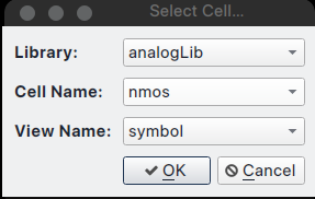
Symbol selection dialogue only displays the symbol views. Choose the desired symbol and
click OK button and click anywhere on the symbol editor window. The symbol will placed at that
point. Note that [@instName] label will be converted to an instance name that starts with **I
** and ends with a unique number. If any of other NLPLabels have a default definition, they will be used. For NLPLabels without a default definition and PyLabels only the definition of the label will be shown.
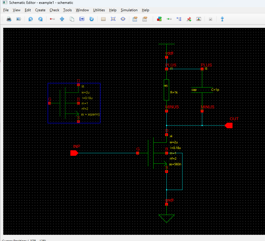
Now the select the instance and press q button to display ==instance properties== dialogue.
Note that as parameter has asparm() shown as its value. Because it is defined as PyLabel in the
symbol, once the values for other labels, e.g. w, l, nf and m are defined, its value
will be calculated according to the formula defined in callbacks.py file.
Note that symbol attributes are also shown under Instance Attributes heading. However, the user cannot edit them using this dialogue, it is just there to inform the designer.

At the moment, only instance name, location and angle can be changed as well as instance label values.
If a schematic is opened but one or more instances cannot be found among the design libraries, a grey box with the missing instance path including library name, cell name and cellview name will be shown.
Creating Wires
Wires are used to make connections between instances at pins. A wire can be created by
pressing w key or selecting Create Wire menu item under Create menu or by clicking toolbar
button.
Wire starts at first point the right mouse button is released after pressing it and ends where it is released after second mouse right button press1
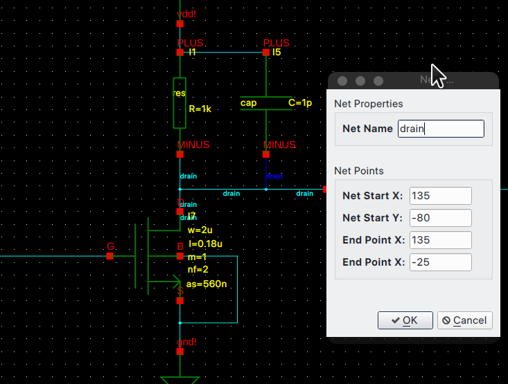
For each net, a net name can be defined using Net Properties dialogue. This name will also
propagate all other wires that wire touches.
If a wire is extended by drawing another wire along its direction, i.e. horizontal or vertical, those wires will be merged and will become a single wire. If two wires are connected such that one wire is orthogonal to the other and connects at a mid-point, a solder-dot will be placed and the wire will be split at the solder dot location.
Net Highlighting
The circuit designers occasionally needs to see which net is connected to other nets as the nets might be connected by name which is not immediately obvious on the schematic. In that case, the user can select Tools->Highlight Net menu item. It is a checkable menu item, and as long as it is checked, net highlighting mode will be effective.
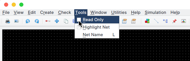
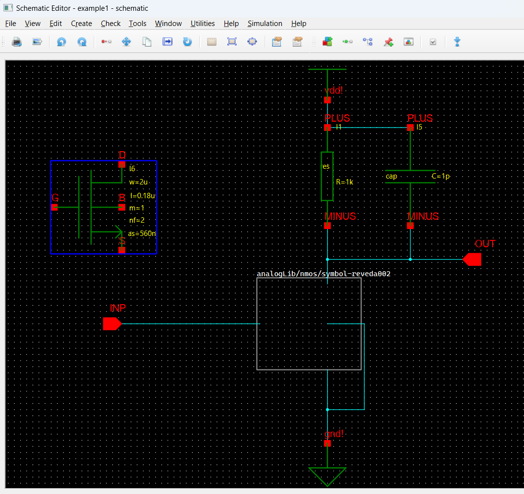
If the mouse cursor hovers on a net, all the nets connected to that net will be highlighted including visual paths connecting centre points of the nets:
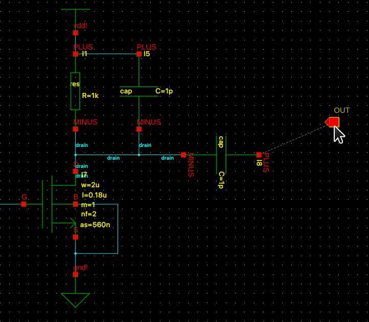
Creating Pins
Like symbol pins, schematic pins define the connection points for the circuit in a hierarchical
design. A pin can be created by pressing p key or selecting relevant menu item or toolbar
button. Pins can have three directions:
- Input
- Output
- InOut
At the moment, Pin Type definition is not used.
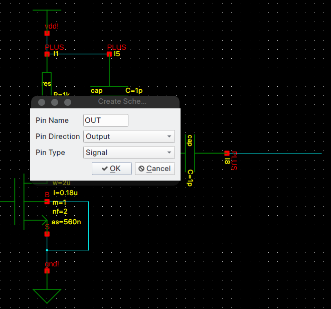
Schematic pins will snap to nets if any nets are connected. If the pin is moved, the connected nets will rearrange to keep the connection.
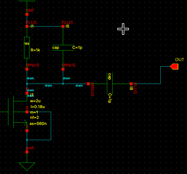
Creating Text
Texts can be placed on the schematics. All monospaced fonts on the system can be used. Software will try to find the closest font if it can not find the exact font when the schematic were to be used in another system. Text Entry dialogue allows the all the available style and sizes of a font to be selected.
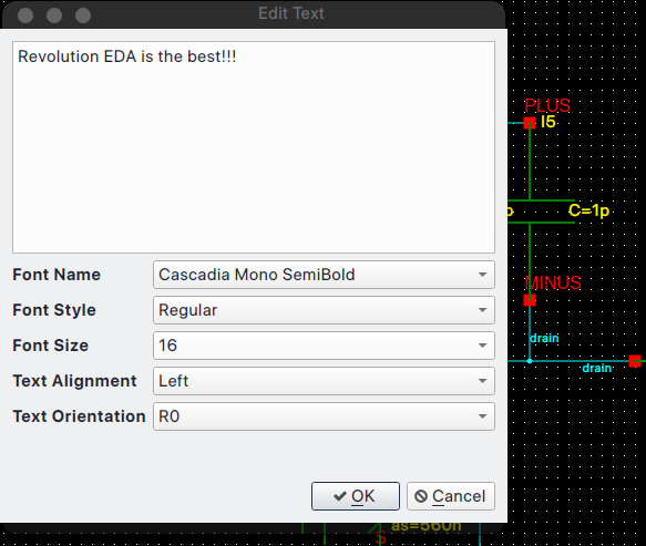
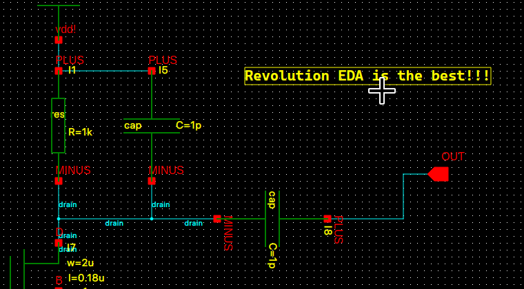
Text orientation can also be changed to rotate the text.
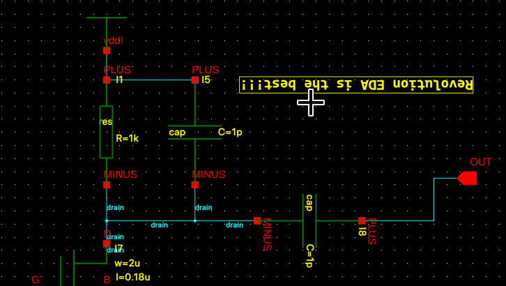
If a text is selected and its property window is brought up using q key, all these properties can also be changed later.
Creating Symbols
A symbol for a schematic can be created automatically using Create Symbol menu item.
Revolution EDA first verify the name of the symbol cell view. As explained earlier, the cell
view name should include symbol in the text. To generate a symbol for a schematic, make sure that all the pins for the symbol defined using schematic pins in the schematic. Then, select Create->Create Symbol... menu item which will bring up symbol creation dialogue:
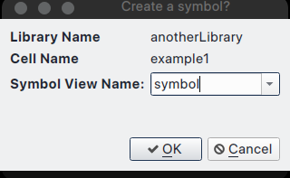
Once the symbol view name is entered, click OK. If a view with the same name exists, the
Revolution EDA will confirm the designer wants to overwrite that view. If the input to that
dialogue is also OK, a new dialogue will be displayed:
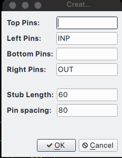
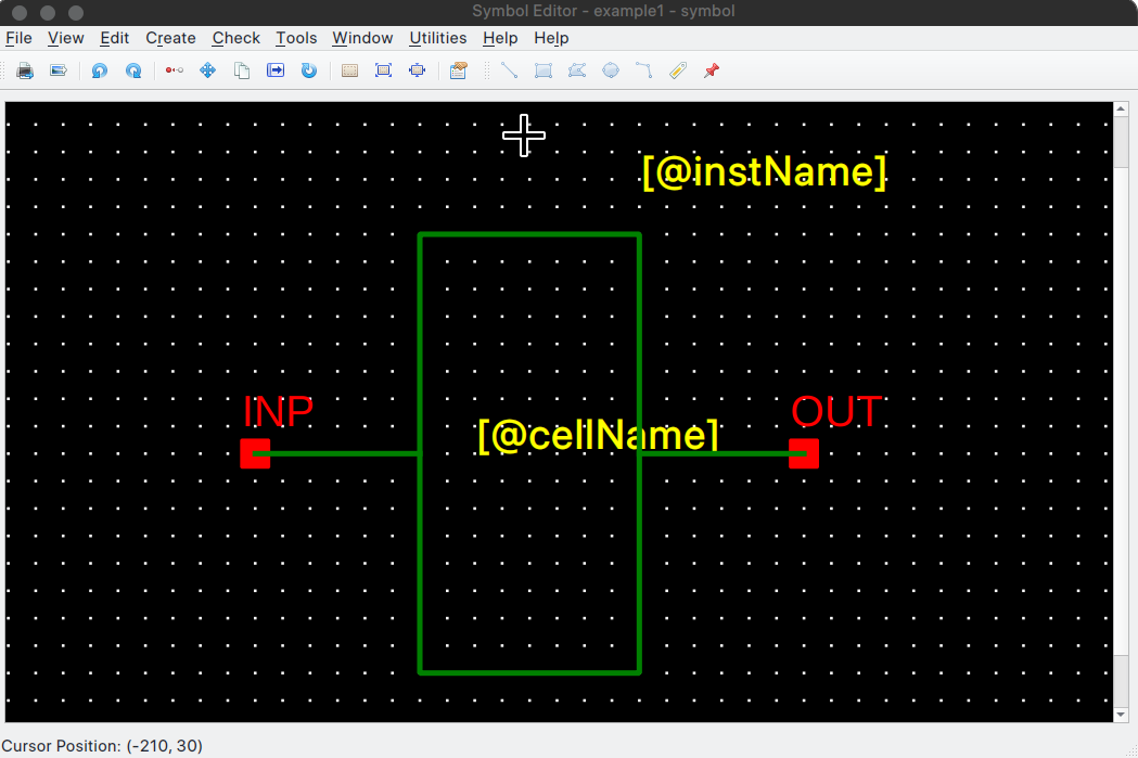
The initial placement of pins is according to their directions. The designer is free to change the location of pins. It is advisable to keep Stub Length and Pin spacing values to keep a consistent look. Once the designer is satisfied the pin locations and symbol geometry parameters, he/she can proceed to creating a symbol view. The symbol view will be opened in another window. A library browser will also show a symbol view is added to the relevant cell.
We have already explained which attributes are necessary for netlisting a symbol depending on the symbol, veriloga or spice cellview, if they exist, would be used for netlisting when needed.
Creating Netlists
Netlist creation can be done through Simulation menu and Create Netlist menu item. It will
start an Export Netlist dialog. Depending on the availability of schematic and config
views, there could be more than one option to choose for view combobox. Here we will be
concentrating on using Switch view list field to control the netlisting process. Once we
explain the config view and the associated editor, we will also touch use of config views in
netlisting process.
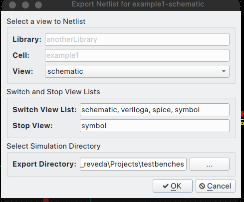
In this dialogue, the view to be netlisted is schematic. Switch view list is the order of preference in netlisting a cell. If a cell has both veriloga and schematic views, schematic view will be preferred and veriloga will not be used. Stop view list defines the views that netlister should not go down in hierarchy. At the moment, only “symbol” view entry is valid.
Export directory field determines the parent folder name for the simulations. It is normally entered at Options menu of main window.
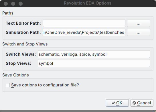
However it could be changed at export netlist field as well. However, it ==will not be saved== in the Revolution EDA configuration file unlike the entries in Options dialogue.
When OK button is clicked,Revolution EDA will do a full hierarchical netlisting of the
circuit. Unlike the leading electronic design automation software, the ==netlisting process will not block the software and the user can continue to work== as normal. The circuit netlist will be placed under SimulationPath/cellName/viewName directory. The
netlist file name will be celllName_viewName.cir where cellName and viewName will be the
cell name and view name of the netlisted circuit. The circuit netlist will like this:
**********************************************************************************
** Revolution EDA CDL Netlist
** Library: anotherLibrary
** Top Cell Name: example2
** View Name: schematic
** Date: 2024-03-16 21:25:51.028310
**********************************************************************************
*.GLOBAL gnd!

XI0 example1 net0 intNoe
.SUBCKT example1 INP  OUT
CI8 OUT drain 1p 0
CI5 net0 drain 1p 0
MI7 drain INP gnd! gnd! nmos w=2u l=0.18u nf=2  as=560n m=1
Yres I1 net0 drain  resModel 1k
.ENDS
XI1 example1 intNoe net1
Yres I4 net1 gnd!  resModel 1k
VI2 net0 gnd! PULSE( 1 1m 1k 0 0 0  )
.END
.MODEL resModel res R = 1
*.HDL /home/eskiyerli/OneDrive_reveda/Projects/RevEDA/exampleLibraries/analogLib/resVa/res.va
Note that verilog-a model is used for the resistor, because veriloga view is before symbol view in the switch view list field. Let’s now reverse their positions and check the output netlist:
**********************************************************************************
** Revolution EDA CDL Netlist
** Library: anotherLibrary
** Top Cell Name: example2
** View Name: schematic
** Date: 2024-03-16 21:34:45.647943
**********************************************************************************
*.GLOBAL gnd!

XI0 example1 net0 intNoe
.SUBCKT example1 INP  OUT
RI1 net0 drain 1k
MI7 drain INP gnd! gnd! nmos w=2u l=0.18u nf=2  as=560n m=1
CI8 OUT drain 1p 0
CI5 net0 drain 1p 0
.ENDS
XI1 example1 intNoe net1
RI4 net1 gnd! 1k
VI2 net0 gnd! PULSE( 1 1m 1k 0 0 0  )
.END
Now the resistor is netlisted as a symbol using the attributes relevant to symbol netlisting, i.e. XyceSymbolNetlistLine and pinOrder.
Ignoring Instances
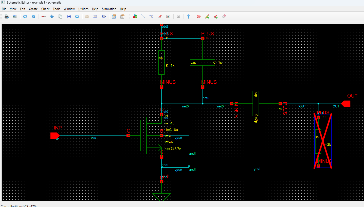
Circuit designers might need netlisting process to ignore some components depending on the testbench purpose. It is very easy to mark instances to be ignored in the netlisting by selecting ignore item in instance context menu. Just select the instance you want to be ignored in the netlisting process and click right mouse button to bring up instance context menu:

ignore menu item is used to toggle if this device instance will be ignored during netlisting. If the user selects it once, a red cross on the instance symbol is drawn. If the user selects an ignored instance and selects the ignore menu item, the red-cross will be removed and symbol instance will be netlisted normally.
Netlister will report the ignored block with a comment as shown in the following netlist for the schematic above, helping the design engineer to make sure that the correct netlist is being used for simulations.
**********************************************************************************
** Revolution EDA CDL Netlist
** Library: anotherLibrary
** Top Cell Name: example1
** View Name: schematic
** Date: 2024-03-19 09:44:44.926891
**********************************************************************************
*.GLOBAL gnd!

CI8 OUT net0 2p 0
MI7 net0 INP gnd! gnd! nmos w=4u l=0.18u nf=6  as=746.7n m=1
*I9 is marked to be ignored
RI1 vdd! net0 1k
CI5 net1 net0 1p 0
.END
Hierarchy Traversing
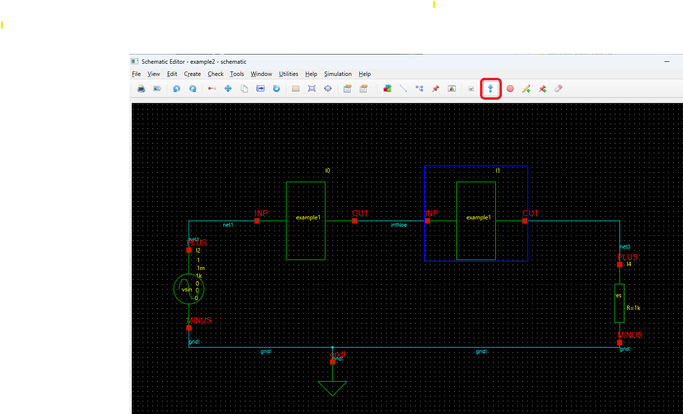
Another functionality provided by Revolution EDA is the hierarchy traversing up and down. For example a design engineer can start editing a schematic and decide to edit the schematic of one of the symbols and in the schematic. By using hierarchy traversing function, it is very easy. At the moment, this function is only available for schematic and symbol views but it will be expanded to other cellviews shortly.
Select a symbol, and do one of these:
- Press on
Go Downbutton on the toolbar, - Select
Edit->Hierarchy->Go Downmenu item, - Press
Shift+Ekey combination, - Right click on mouse to pop up the context menu and select
Go Downentry
A dialogue titled Go Down Hieararchy will pop up. Depending on the cell, you could choose Symbol or Schematic view to open either in edit or read-only mode.
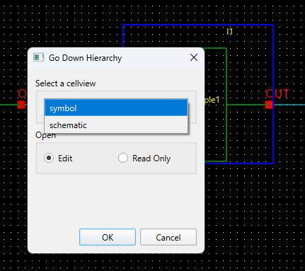
Assuming the symbol is opened for editing, the designer could save the symbol after finishing the edits and now choose Go Up button on the toolbar to close the window. The changes in the symbol will be reflected in the original schematic.
-
This behaviour is different than the behaviour in version 0.5 series. ↩